 |
|
|
|
|
|
|
|
|
|
|
|
|
|
|
|
|
|
|
|
|
|
|
|
|
|
|
|
|
VUTRAX Design Integrity
Design Checking
 Provides dual checking of logical connectivity with
both on-line and off-line checking for dimensional clearances.
Provides dual checking of logical connectivity with
both on-line and off-line checking for dimensional clearances.
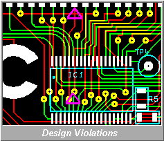
All artwork elements may be cross-checked and warnings given both as a report and on screen highlight. Groups of signals may be defined with differing clearance rules within the group or to alternate groups, and different clearances assigned to pads, tracks etc. each on different layers.
The final interconnect is checked against the original rats-nest (unrouted interconnect) to ensure that no error by the user or 3rd party processing modules has introduced any errors.
Forward (Top-Down) Modification
Fundamental changes to the electronics that are initiated on the schematic are reflected at any stage into the current artwork. Deleted nets can still be used as templates for new routes or plotted as part of a salvage scheme for on-site service.
Backwards Modification
All gate and pin swops and any silkscreen changes on the PCB are reflected graphically and textually back to the schematic. Complicated changes beyond the possibilities of automatic update to the schematic are detected and reported.
EMC Compatibility Assessment
The EMC (Electromagnetic Compatibility) checker analyses the PCB layout and circuit elements looking for characteristics that may cause problems in satisfying the EC EMC directives.
The facility is rule driven to allow the intensity to be adjusted according to the environment in which the board is to operate.
Key features checked include
- Examines the configuration of tracks (traces) and reports single or sequences of connections that may form a significant antenna.
- Special attention of areas near resonators.
- Improper connection between multiple (e.g. digital and analogue) grounds.
- Improper connections to split powerplanes.
- Violation of the specified type of power decoupling.
- Noisy or susceptable signals near the edge of the board.
- External connections without static protection.