|
|
|
|
|
|
|
|
|
|
|
|
|
|
|
|
|
|
|
|
|
|
|
|
|
|
|
|
|
|
VUTRAX Schematic Entry
Component & Footprint Libraries
There are thousands of logical library symbols including connectors (DIN, D-type, IDC etc), various assorted linear and discrete devices, CMOS, 74 Series and microprocessors.
Physical parts (imperial or metric) include common outlines such as DIL packages, small-outline and leadless chip carriers...and any footprint and symbol can be defined explicitly.
An unusual feature of VUTRAX is that the schematic does not have to be modified if the packaging style is changed. Pin numbering changes are transfered back to the schematic by the back-annotation facilities.
Schematic Capture
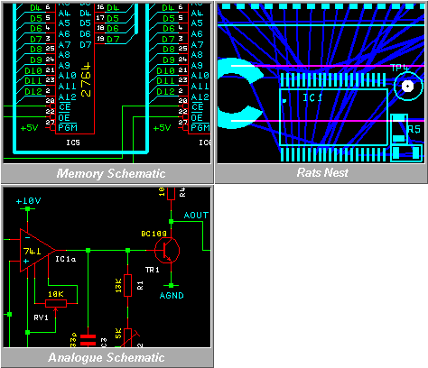
Quickly creates accurate circuit data by drawing lines or applying signal names to interconnect components copied from the library. For multi-station projects, designs can be partitioned so each designer can work independently. The design, device and connection data can be subsequently extracted from the circuits and verified using digital or analogue simulation before passing on to PCB layout.
Schematic Capture will also check for unconnected device pins and add "T" junction markers. The Back Annotation/Modify facilities will automatically add pin numbers and component references for use on the PCB.
Rat's Nest Generator
 Connection data, library data and track widths are processed and
various checks performed. Gates used on the schematic are
packaged into physical devices on the PCB.
From this information the system creates a Rat's Nest (a screen display of all the components in a "tray", with point-to-point connections between them). The process also generates a parts list, engineer's check list and comprehensive tabulated data for post processing to simulation, pick & place and ATE.
Component Placement
Components in a Rat's Nest are placed manually or automatically by moving them from the "tray" on to the board profile. They can be rotated and/or flipped to the other side of the board.
To help show where components should be placed, "Dynamic Component Connection Banding" illustrates the nearest connection to each component pad when components are moved. Also, a Histogram displays connection densities across the PCB.
Signals can be flashed individually or by component to identify the pins they visit. At any time during placement, the signal paths can be optimised to the shortest route between points. Gates and pins may be swapped to reduce "crossovers". You can also select special optimisations for signals and for power connections, including options for ECL logic.